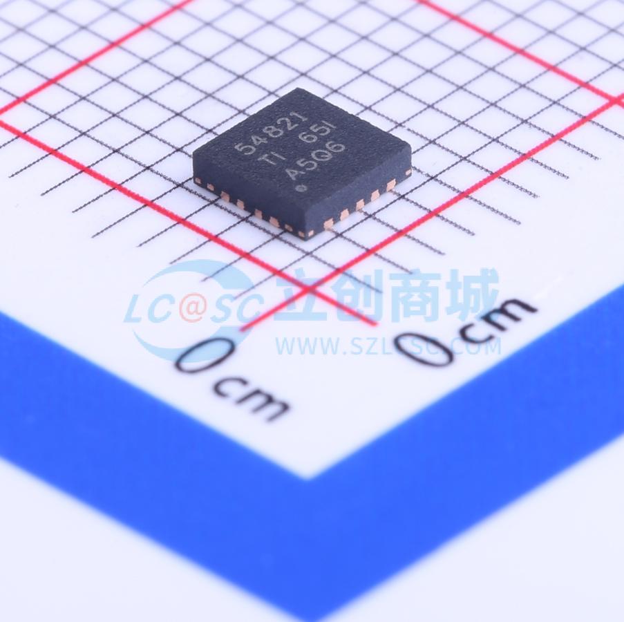
商品参数
| 属性 | 参数值 | |
|---|---|---|
| 商品目录 | DC-DC电源芯片 | |
| 功能类型 | 降压型 | |
| 工作电压 | 4.5V~17V | |
| 输出电压 | 600mV~15V | |
| 输出电流 | 8A | |
| 开关频率 | 1.6MHz | |
| 工作温度 | -40℃~+125℃@(TJ) |
| 属性 | 参数值 | |
|---|---|---|
| 同步整流 | 是 | |
| 输出通道数 | 1 | |
| 拓扑结构 | 降压式 | |
| 静态电流(Iq) | 600uA | |
| 开关管(内置/外置) | 内置 | |
| 输出类型 | 可调 |
商品概述
采用耐热性能增强型3.5毫米×3.5毫米QFN封装的TPS54821是一款全功能17 V、8 A同步降压转换器。凭借高效率和集成高侧/低侧MOSFET,此降压器为适应小型设计要求而进行了优化。通过电流模式控制减少组件数量,并通过选择高开关频率缩小电感器占位面积,从而可进一步节省空间。
输出电压启动斜线上升由SS/TR引脚控制,其操作既支持独立电源供电模式又支持跟踪模式。通过正确配置使能引脚与漏极开路电源状态正常引脚也可实现电源排序。
高侧FET的逐周期电流限制可在过载情况下保护器件不受损害,并可通过使用避免电流击穿的低侧源电流限制来增强此功能。此外,还有一个可关闭低侧MOSFET的低侧吸收电流限制以防止过大的反向电流。在过载电流情况持续时间超过预设时间时,断续保护功能将被触发。当裸片温度超过热关断温度时,过热断续保护功能将禁用该器件,而在内置热关断断续时间之后,该部件会被重新启用。
The device is a 17-V, 8-A, synchronous step-down (buck) converter with two integrated n-channel MOSFETs. To improve performance during line and load transients the device implements a constant frequency, peak current mode control which also simplifies external frequency compensation. The wide switching frequency of 200 kHz to 1600 kHz allows for efficiency and size optimization when selecting the output filter components. The switching frequency is adjusted using a resistor to ground on the RT/CLK pin. The device also has an internal phase lock loop (PLL) controlled by the RT/CLK pin that can be used to synchronize the switching cycle to the falling edge of an external system clock.
The device has been designed for safe monotonic startup into pre-biased loads. The default start up is when VIN is typically 4.0 V. The EN pin has an internal pull-up current source that can be used to adjust the input voltage under voltage lockout (UVLO) with two external resistors. In addition, the EN pin can be floating for the device to operate with the internal pull-up current. The total operating current for the device is approximately 600 μA when not switching and under no load. When the device is disabled, the supply current is typically less than 2 μA.
The integrated MOSFETs allow for high efficiency power supply designs with continuous output currents up to 8 amperes. The MOSFETs have been sized to optimize efficiency for lower duty cycle applications.
The device reduces the external component count by integrating the boot recharge circuit. The bias voltage for the integrated high-side MOSFET is supplied by a capacitor between the BOOT and PH pins. The boot capacitor voltage is monitored by a BOOT to PH UVLO (BOOT-PH UVLO) circuit allowing PH pin to be pulled low to recharge the boot capacitor. The device can operate at 100% duty cycle as long as the boot capacitor voltage is higher than the preset BOOT-PH UVLO threshold which is typically 2.1V. The output voltage can be stepped down to as low as the 0.6V voltage reference (Vref).
The device has a power good comparator (PWRGD) with hysteresis which monitors the output voltage through the VSENSE pin. The PWRGD pin is an open drain MOSFET which is pulled low when the VSENSE pin voltage is less than 92% or greater than 106% of the reference voltage Vref and asserts high when the VSENSE pin voltage is 94% to 104% of the Vref.
The SS/TR (slow start/tracking) pin is used to minimize inrush currents or provide power supply sequencing during power up. A small value capacitor or resistor divider should be coupled to the pin for slow start or critical power supply s
商品特性
- 集成式±26 mΩ / 19 mΩ MOSFET
- 分离电源轨:1.6 V至17 V的PVIN
- 200 kHz至1.6 MHz开关频率
- 与外部时钟同步
- 不同温度下基准电压为0.6 V ±1%
- 2 μA的低关断静态电流
- 单调启动至预偏置输出
- 工作结点温度范围:-40℃至125℃
- 可调慢启动/电源时序
- 针对欠压及过压的功率正常输出监控
- 可调输入欠压闭锁
应用领域
- 数字电视电源
- 机顶盒
- 蓝光DVD
- 家用终端高性能负载点稳压设计

