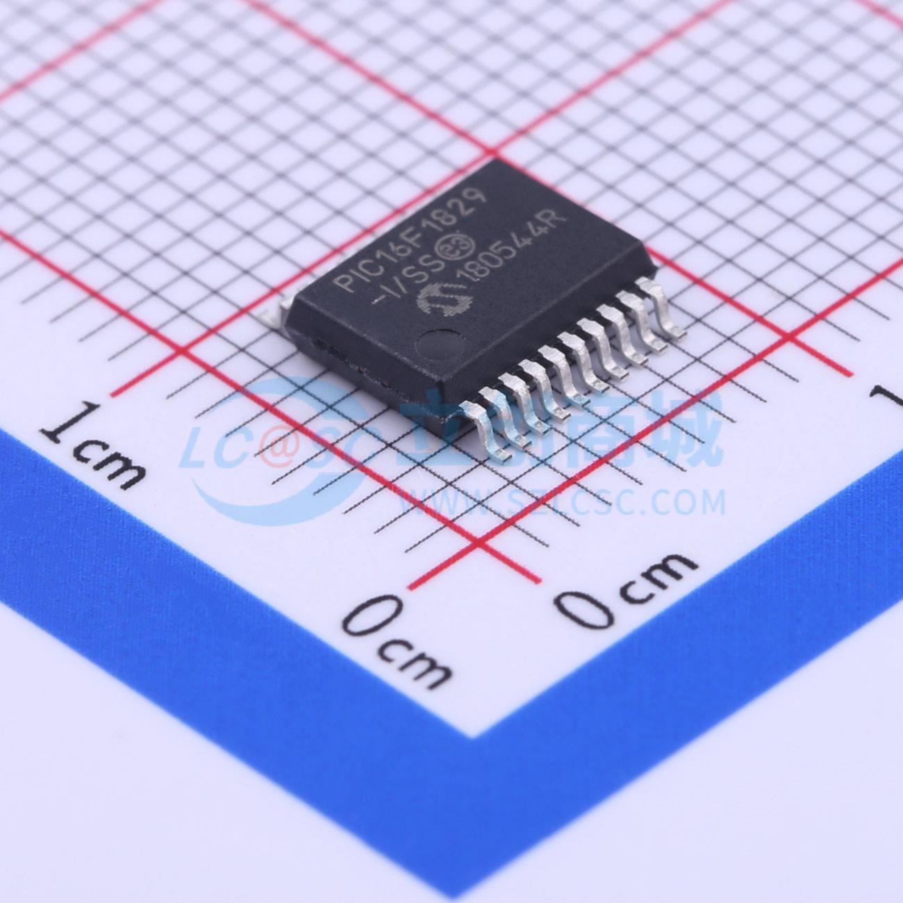
PIC16F1829-I/SS
采用XLP技术的14/20引脚闪存微控制器
SMT扩展库PCB免费打样
私有库下单最高享92折
- 描述
- 特性:高性能RISC CPU:仅需学习49条指令,除分支指令外均为单周期指令。工作速度:直流-32 MHz振荡器/时钟输入,直流-125 ns指令周期。高达16 Kbytes线性程序存储器寻址。高达1024 bytes线性数据存储器寻址。具备自动上下文保存的中断能力。16级深度硬件堆栈,可选溢出/下溢复位。直接、间接和相对寻址模式,两个完整的16位文件选择寄存器(FSRs),FSRs可读取程序和数据存储器。 灵活的振荡器结构:精密32 MHz内部振荡器模块,工厂校准至±1%(典型值),软件可选频率范围为31 kHz至32 MHz
- 品牌名称
- MICROCHIP(美国微芯)
- 商品型号
- PIC16F1829-I/SS
- 商品编号
- C36311
- 商品封装
- SSOP-20-208mil
- 包装方式
- 管装
- 商品毛重
- 0.358克(g)
商品参数
| 属性 | 参数值 | |
|---|---|---|
| 商品目录 | 单片机(MCU/MPU/SOC) | |
| CPU内核 | PIC | |
| CPU最大主频 | 32MHz | |
| CPU位数 | 8 Bit | |
| 程序存储容量 | 14KB | |
| 程序存储器类型 | FLASH | |
| RAM容量 | 1KB |
| 属性 | 参数值 | |
|---|---|---|
| EEPROM容量 | 256Byte | |
| I/O数量 | 17 | |
| ADC(位数) | 10bit | |
| 振荡器类型 | 内置 | |
| 工作电压 | 1.8V~5.5V | |
| 工作温度 | -40℃~+85℃ | |
| 功能特性 | 堆栈溢出复位;欠压检测(BOR/LVD/LVR/LVI);上电复位(POR);看门狗复位;内置通用定时器;触控功能;软件复位 |
商品特性
- Only 49 Instructions to Learn: All single-cycle instructions except branches
- Operating Speed: DC – 32 MHz oscillator/clock input, DC – 125 ns instruction cycle
- Up to 16 Kbytes Linear Program Memory Addressing
- Up to 1024 bytes Linear Data Memory Addressing
- Interrupt Capability with Automatic Context Saving
- 16-Level Deep Hardware Stack with Optional Overflow/Underflow Reset
- Direct, Indirect and Relative Addressing modes: Two full 16-bit File Select Registers (FSRs), FSRs can read program and data memory
- Precision 32 MHz Internal Oscillator Block: Factory calibrated to ± 1%, typical, Software selectable frequencies range of 31 kHz to 32 MHz
- 31 kHz Low-Power Internal Oscillator
- Four Crystal modes up to 32 MHz
- Three External Clock modes up to 32 MHz
- 4x Phase Lock Loop (PLL)
- Fail-Safe Clock Monitor: Allows for safe shutdown if peripheral clock stops
- Two-Speed Oscillator Start-Up
- Reference Clock Module: Programmable clock output frequency and duty cycle
- 1.8V - 5.5V Operation – PIC16F1825/9
- 1.8V - 3.6V Operation – PIC16LF1825/9
- Self-Programmable under Software Control
- Power-on Reset (POR), Power-up Timer (PWRT) and Oscillator Start-up Timer (OST)
- Programmable Brown-out Reset (BOR)
- Extended Watchdog Timer (WDT)
- In-Circuit Serial Programming via Two Pins
- In-Circuit Debug (ICD) via Two Pins
- Enhanced Low-Voltage Programming (LVP)
- Programmable Code Protection
- Power-Saving Sleep mode
- Sleep mode: 20 nA × 1.8V, typical
- Watchdog Timer: 300 nA α↑.8V, typical
- Timer1 Oscillator: 650 nA ⨂ 32 kHz, 1.8V, typical
- Operating Current: 48 μA/MHz ⓐ (ω).8V, typical
- Analog-to-Digital Converter (ADC) Module: 10-bit resolution, up to 12 channels, Auto acquisition capability, Conversion available during Sleep
- Analog Comparator Module: Two rail-to-rail analog comparators, Power mode control, Software controllable hysteresis
- Voltage Reference Module: Fixed Voltage Reference (FVR) with 1.024V, 2.048V and 4.096V output levels, 5-bit rail-to-rail resistive DAC with positive and negative reference selection
- Up to 17 I/O Pins and 1 Input Only Pin: High current sink/source 25 mA/25 mA, Programmable weak pull-ups, Programmable interrupt-on-change pins
- Timer0: 8-Bit Timer/Counter with 8-Bit Prescaler
- Enhanced Timer1: 16-bit timer/counter with prescaler, External Gate Input mode, Dedicated, low-power 32 kHz oscillator driver
- Three Timer2-types: 8-Bit Timer/Counter with 8-Bit Period Register, Prescaler and Postscaler
- Two Capture, Compare, PWM (CCP) Modules
- Two Enhanced CCP (ECCP) Modules: Software selectable time bases, Auto-shutdown and auto-restart, PWM steering
- Up to Two Master Synchronous Serial Port (MSSP) with SPI and I²C with: 7-bit address masking, SMBus/PMBus compatibility
- Enhanced Universal Synchronous Asynchronous Receiver Transmitter (EUSART) Module
- mTouch Sensing Oscillator Module: Up to 12 input channels
- Data Signal Modulator Module: Selectable modulator and carrier sources
- SR Latch: Multiple Set/Reset input options, Emulates 555 Timer applications
相似推荐
其他推荐
- AT91SAM7X256C-AU
- PIC10F222T-I/OT
- PIC16F639-I/SS
- PIC16F886-I/SS
- ATMEGA644PA-AU
- PIC16F1947-I/PT
- PIC18LF4550T-I/PT
- AT91SAM7S256D-AU
- AT89S52-24JU
- PIC16F74-I/PT
- ATMEGA1281-16AU
- PIC12F1840-I/SN
- PIC18F24k22-I/SO
- PIC16LF1503-I/SL
- AT91SAM9G20B-CU
- ATTINY13A-SSUR
- PIC16F886-I/SO
- PIC16F883-I/SO
- AT91M40800-33AU
- PIC16F627A-I/SO
- PIC16F1939-I/PT

