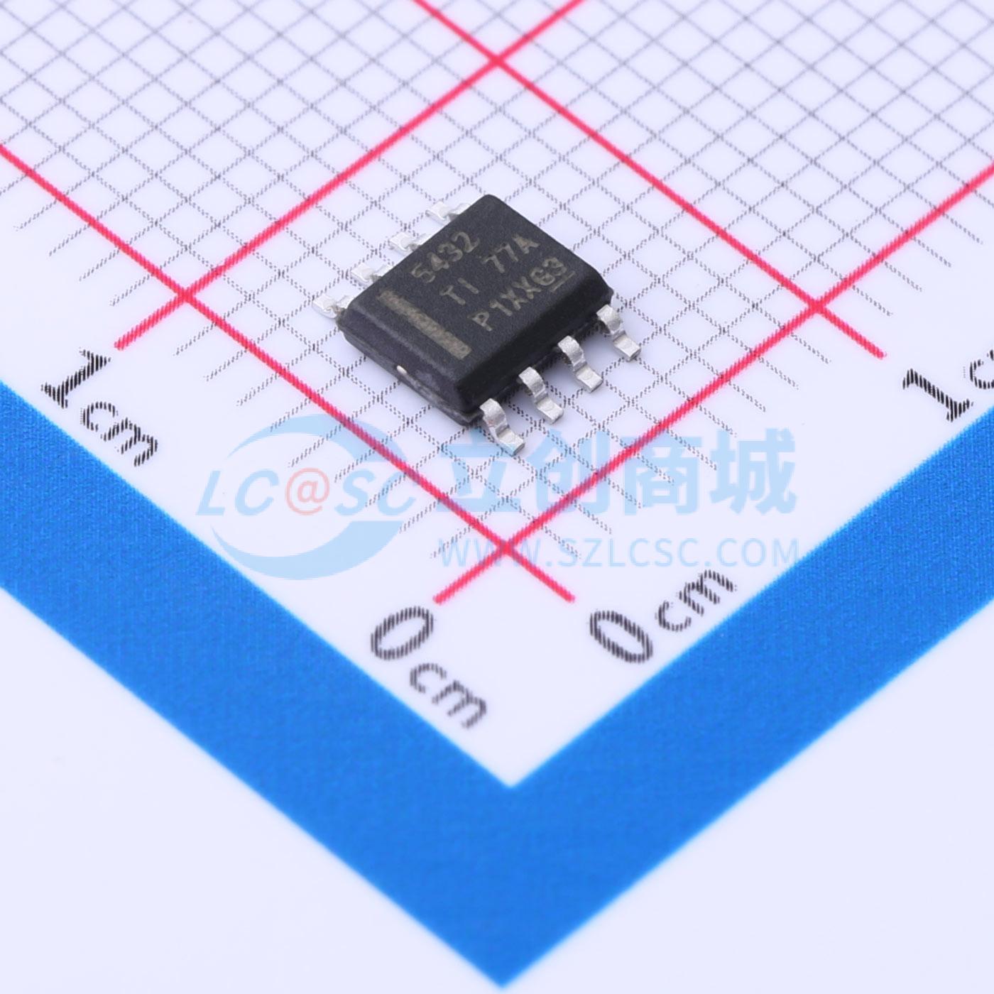
TPS5432DDA
降压型 3A 2.95V~6V
- 描述
- TPS5432是一款6V,3A,低静态电流,电流模式,同步单片降压转换器,具有700kHz的固定开关频率。集成MOSFET,外部补偿,电流模式控制,360uA无负载静态工作电流,0.808V内部电压基准,25°C时基准精度为±2.0%,-40°C至125°C温度范围内+3.0%的基准精度。适用于消费类应用,如数字电视、机顶盒、LCD显示器等。
- 品牌名称
- TI(德州仪器)
- 商品型号
- TPS5432DDA
- 商品编号
- C1355861
- 商品封装
- SO-8
- 包装方式
- 管装
- 商品毛重
- 0.65克(g)
商品参数
| 属性 | 参数值 | |
|---|---|---|
| 商品目录 | DC-DC电源芯片 | |
| 功能类型 | 降压型 | |
| 工作电压 | 2.95V~6V | |
| 输出电压 | 808mV~4.5V | |
| 输出电流 | 3A | |
| 开关频率 | 700kHz | |
| 工作温度 | -40℃~+125℃@(TJ) |
| 属性 | 参数值 | |
|---|---|---|
| 同步整流 | 是 | |
| 输出通道数 | 1 | |
| 拓扑结构 | 降压式 | |
| 静态电流(Iq) | - | |
| 开关管(内置/外置) | 内置 | |
| 输出类型 | 可调 |
商品概述
TPS5432是一款带有集成型MOSFET的6V,3A,低静态电流(Iq),电流模式,同步单片降压转换器。 TPS5432通过集成MOSFET、执行电流模式控制来实现小型设计,从而减少外部组件数量、使用700kHz开关频率来减小电感器尺寸。带有外露散热垫的SOIC - 8封装方式提供耐热增强型解决方案并且易于使用。 TPS5432在温度范围内提供带有精确电压基准(3.0%)的针对多种负载的准确调节。 通过集成的70mΩ MOSFET和典型值为360μA的电源电流,效率得以大幅提升。通过使用使能引脚进入关断模式,关断电流可减少至2μA。 输出电压启动斜坡由慢启动引脚控制。一个位于此引脚上的陶瓷电容器可以很容易的调节慢启动时间。 频率折返和热关断功能在过流情况下保护器件不受损坏。
The TPS5432 is a 6 - V, 3 - A, synchronous step - down (buck) converter with two integrated n - channel MOSFETs. To improve performance during line and load transients the device implements a constant frequency, peak current mode control which reduces output capacitance and simplifies external frequency compensation design. The fixed switching frequency of 700kHz provides the balance between efficiency and size of the output filter components. The TPS5432 has a typical default start up voltage of 2.6 V. The EN pin has an internal pull - up current source that can provide a default condition when the EN pin is floating for the device to operate. The total operating current for the TPS5432 is typically 360μA when not switching and under no load. When the device is disabled, the supply current is less than 5μA. The integrated 70mΩ MOSFETs allow for high efficiency power supply designs with continuous output currents up to 3 amperes. The TPS5432 reduces the external component count by integrating the boot recharge diode. The bias voltage for the integrated high side MOSFET is supplied by a capacitor between the BOOT and PH pins. The boot capacitor voltage is monitored by an UVLO circuit and turns off the high side MOSFET when the voltage falls below a preset threshold. The output voltage can be stepped down to as low as the 0.808 V reference. The TPS5432 minimizes excessive output over - voltage transients by taking advantage of the over - voltage comparator. When the regulated output voltage is greater than 107% of the nominal voltage, the over - voltage comparator is activated, and the high side MOSFET is turned off and masked from turning on until the output voltage is lower than 105%. The SS (slow start) pin is used to minimize inrush currents during power up. A small value capacitor should be coupled to the pin for slow start. The SS pin is discharged before the output power up to ensure a repeatable restart after an over - temperature fault, UVLO fault or disabled condition. The use of a frequency fold - back circuit reduces the switching frequency during startup and over current fault conditions to help limit the inductor current.
商品特性
- 两个用于生成3A持续输出电流的70mΩ(典型值)场效应管(MOSFET)
- 带有外部补偿的电流模式控制
- 700kHz开关频率
- 360μa无负载静态工作电流(没有开关)
- 内部电压基准为0.808V
- 25°C时,基准精度为±2.0%
- -40°C - 125°C温度范围内±3.0%的基准精度
- 与陶瓷输出电容器一起工作时保持稳定运行
- 可调节慢启动
- 逐周期电流限制、和频率折返保护功能
- 耐热增强型8引脚小外形尺寸集成电路(SOIC)(DDA)封装
应用领域
- 诸如数字电视(DTV)、机顶盒、LCD显示器、用户端设备(CPE)的消费类应用
- 针对片上系统(SoC),CPU,数字信号处理器(DSP)的低压负载点调节

