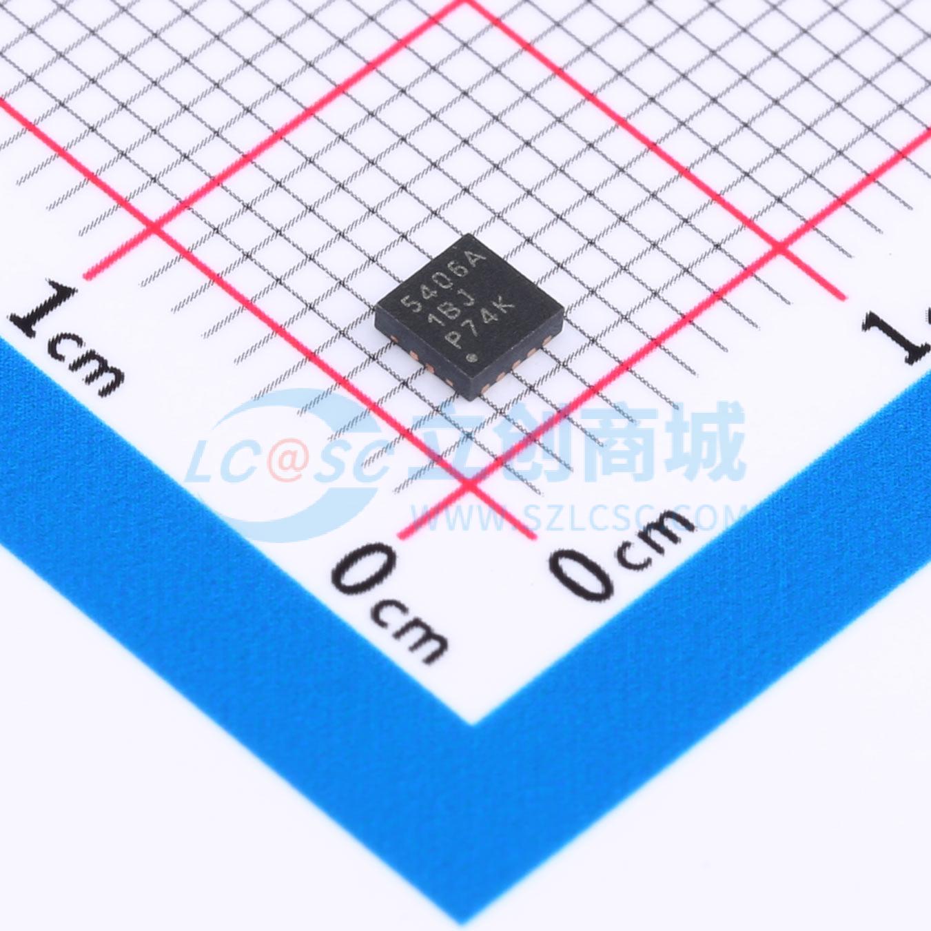
TPS54060ADRCR
降压型 500mA 3.5V~60V
- 描述
- TPS54060A 具有 Eco-Mode 的 3.5V 至 60V 输入、0.5A 降压转换器
- 品牌名称
- TI(德州仪器)
- 商品型号
- TPS54060ADRCR
- 商品编号
- C544684
- 商品封装
- VSON-10(3x3)
- 包装方式
- 编带
- 商品毛重
- 0.18克(g)
商品参数
| 属性 | 参数值 | |
|---|---|---|
| 商品目录 | DC-DC电源芯片 | |
| 功能类型 | 降压型 | |
| 工作电压 | 3.5V~60V | |
| 输出电压 | - | |
| 输出电流 | 500mA | |
| 开关频率 | 2.5MHz | |
| 工作温度 | -40℃~+150℃@(TJ) |
| 属性 | 参数值 | |
|---|---|---|
| 同步整流 | 否 | |
| 输出通道数 | 1 | |
| 拓扑结构 | 降压式 | |
| 静态电流(Iq) | 116uA | |
| 开关管(内置/外置) | 内置 | |
| 输出类型 | 可调 |
商品概述
TPS54060A器件是一款带有集成型高侧MOSFET的60V,0.5A,降压稳压器。电流模式控制提供了简单的外部补偿和组件选择的灵活性。一个低纹波脉冲跳跃模式将无负载的稳定输出电源电流减小至116μA。采用使能引脚可将停机模式的电源电流降低至1.3μA(此时,使能引脚为低电平)。 欠压闭锁在内部设定为2.5V,但可采用使能引脚将之提高。输出电压启动斜坡受控于缓慢起动引脚,该引脚还可以通过配置来控制排序/跟踪。一个开漏电源正常信号表示输出在94%至107%的范围内。 宽开关频率范围允许对效率及外部组件尺寸进行优化。频率折返和热关断功能在过载情况下对部件实施保护。
The TPS54060A device is a 60-V, 0.5-A, step-down (buck) regulator with an integrated high side n-channel MOSFET. To improve performance during line and load transients the device implements a constant frequency, current mode control which reduces output capacitance and simplifies external frequency compensation design. The wide switching frequency of 100kHz to 2500kHz allows for efficiency and size optimization when selecting the output filter components. The switching frequency is adjusted using a resistor to ground on the RT/CLK pin. The device has an internal phase lock loop (PLL) on the RT/CLK pin that is used to synchronize the power switch turn on to a falling edge of an external system clock. The TPS54060A has a default start up voltage of approximately 2.5V. The EN pin has an internal pull-up current source that can be used to adjust the input voltage under voltage lockout (UVLO) threshold with two external resistors. In addition, the pull up current provides a default condition. When the EN pin is floating the device will operate. The operating current is 116μA when not switching and under no load. When the device is disabled, the supply current is 1.3μA. The integrated 200mΩ high side MOSFET allows for high efficiency power supply designs capable of delivering 0.5 amperes of continuous current to a load. The TPS54060A reduces the external component count by integrating the boot recharge diode. The bias voltage for the integrated high side MOSFET is supplied by a capacitor on the BOOT to PH pin. The boot capacitor voltage is monitored by an UVLO circuit and will turn the high side MOSFET off when the boot voltage falls below a preset threshold. The TPS54060A can operate at high duty cycles because of the boot UVLO. The output voltage can be stepped down to as low as the 0.8V reference. The TPS54060A has a power good comparator (PWRGD) which asserts when the regulated output voltage is less than 92% or greater than 109% of the nominal output voltage. The PWRGD pin is an open drain output which deasserts when the VSENSE pin voltage is between 94% and 107% of the nominal output voltage allowing the pin to transition high when a pull-up resistor is used. The TPS54060A minimizes excessive output overvoltage (OV) transients by taking advantage of the OV power good comparator. When the OV comparator is activated, the high side MOSFET is turned off and masked from turning on until the output voltage is lower than 107%. The SS/TR (slow start/tracking) pin is used to minimize inrush currents or provide power supply sequencing during power up. A small value capacitor should be coupled to the pin to adjust the slow start time. A resistor divider can be coupled to the pin for critical power supply sequencing requirements
商品特性
- 3.5V至60V输入电压范围
- 200mΩ高侧金属氧化物半导体场效应晶体管(MOSFET)
- 在带有脉冲跳跃的轻负载条件上的高效率Eco-mode™
- 比TPS54060更严密的使能阀值以获得更精确的欠压闭锁(UVLO)电压
- 可调的UVLO电压和滞后
- 运行静态电流116μA
- 关断电流1.3μA
- 100kHz至2.5MHz的开关频率同步至外部时钟
- 可调节的缓起动/排序
- 欠压(UV)和过流(OV)电源正常输出
- 0.8V内部电压基准
- 微型小外形尺寸(MSOP)和3mm x 3mm超薄小外形尺寸(VSON)-10封装,这些封装具有PowerPAD™
- 由WEBENCH和SwitcherPro软件工具
应用领域
- 12V,24V和48V工业及商用低功耗系统
- 汽车售后加装配件:视频、全球卫星定位(GPS)、娱乐

